
For this page to display as I would like, please use a resolution of at least 1024 by 768.
Originally this design was made for a computer with a built-in parallel port. Later I bought a new one which had no parallel nor serial ports built in, so I have added a section explaining how to control the camera from a USB port.
I had to start by making some simple decisions. I wanted:
1. Long exposures.
2. Amp off.
3. Cooling.
I decided:
1. To use the pin-lift method exactly as described by Steve Chambers.
I had done this before on a 740
and it wasn't as bad as it seemed, and I didn't fancy cutting and soldering to those tiny tracks.
2. To use the method described by Greg Beeke.
This does not involve lifting legs on the CCD and is, in my view, a nice simple technique.
3. To cool the whole enclosure. This may be inefficient, but I didn't fancy removing the CCD, fixing it to
a cold finger and wiring it back to the circuit board. This is one disadvantage of the ToUcam over the Vesta;
the latter has its CCD on a separate board and cooling just the CCD is a lot easier than the ToUcam where the
CCD is on the same board as the rest of the electronics.
 The new ToUcam 840K is believed to be electrically identical to the 740K, and the circuit board is
undoubtedly identical (it has the same number etched onto it) but it is overprinted '840K' so some components
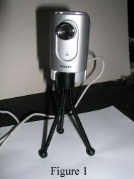
may be different, I don't know. The major difference is the case shown in Figure 1. One nice thing is that
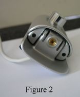
it has a standard tripod bush on the underside, which was lacking in the 740K; the downside is that you can't
screw it to a standard tripod or, I suspect, to afocal supports, because the bush is too close to a part of
the stand used if the little tripod is not used. This can be seen in Figure 2. Not a problem for me, but if
you want to use the camera unmodified afocally, you will have to remove this piece of plastic. The other major
difference is that the USB cable is only half the length of the one on the 740K and more like that on the
Vesta.
The new ToUcam 840K is believed to be electrically identical to the 740K, and the circuit board is
undoubtedly identical (it has the same number etched onto it) but it is overprinted '840K' so some components
may be different, I don't know. The major difference is the case shown in Figure 1. One nice thing is that
it has a standard tripod bush on the underside, which was lacking in the 740K; the downside is that you can't
screw it to a standard tripod or, I suspect, to afocal supports, because the bush is too close to a part of
the stand used if the little tripod is not used. This can be seen in Figure 2. Not a problem for me, but if
you want to use the camera unmodified afocally, you will have to remove this piece of plastic. The other major
difference is that the USB cable is only half the length of the one on the 740K and more like that on the
Vesta.
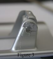
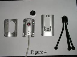
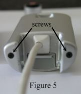
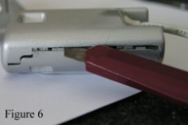
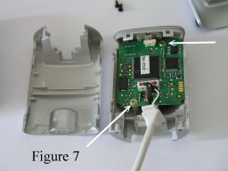
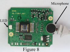
The camera has a decorative cover on the front, which can easily be prised off with a screwdriver or knife inserted behind it. More difficult is the built-in stand without damage. This is because of the way the hinge part is mounded (see Figure 3). If you have no intention of putting the camera back together again, then damage is not a problem, but in any case prising and brute force will eventually get it off. The lens unscrews and you have the parts shown in Figure 4. Next two small screws in the base must be removed (Figure 5) after which the case can be carefully prised apart as shown in Figure 6. If you don't want to break it then try to push the front section inwards to release the catches and slide the back upwards. Figure 7 shows the camera opened up and the two screws that hold the circuit board in place. Remove these and lift out the board (Figure 8). The microphone and the LED can be removed.
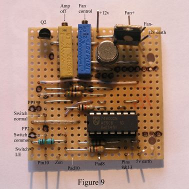
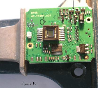
I made a simple circuit board from strip-board for the extra circuitry. This is shown in Figure 9. The circuit diagam is shown in Figure 21 below. The tracks on the back run vertically in the picture, and are broken where a hole is ringed in black. (There may be more under components.) It is electrically divided into three parts, the LE circuitry around the IC, the amp-off circuitry at the top-left, and a circuit to control the speed of the internal fan at the top-right. Note that I had omitted a pin for connection to pad 10 when I took this picture; it was added later. The LE circuit is exactly as shown by Steve Chambers, except that I used a DPDT switch and switched the connection the parallel port as well as that to pin 10. This prevents the parallel port interfering with the camera when switched to normal mode. The Amp-off is that by Greg Beeke except that I used a spare gate in the IC in place of his Q1. The point on the main circuit board where the connection is made for this purpose is shown by an arrow in Figure 10; it connects to the point labelled "Zen" in Figure 9.
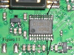 Figure 10 shows the board clamped in a framing clamp ready for modification. It is important to have
the board securely mounted so it doesn't move during the delicate soldering operations. The microphone has
been removed but I removed the LED later. Figure 11 is a closer view of the D16510 chip with the pins
that need to be raised indicated. Undoubtedly the easiest is pin 10 (in the corner) and the hardest pin 13
(on the far side). This isn't as difficult as you might think. You need a very small soldering iron; I
found an old one with a 2 mm bit and filed it down to a sharp point (tinned immediately to reduce oxidation
of the copper). I cut a piece of desoldering tape at an angle to get a sharp pointed end, placed that on the
joint and placed the hot iron on it until the solder melted and ran into the braid. Whilst it is better to
avoid overheating the chip, the joint must get hot enough to melt the solder fully for long enough to wick up
the solder. The pin is still stuck to the pad at this stage. I took a craft knife with a very thin, pointed
blade and inserted it behind the pin. I then reheated the pin with the iron and gently eased the pin up. I think
it is worth always heating the pin when trying to bend it; I believe it is excess solder on the pin that
makes it stiff enough to break. Other people have said the pins are very brittle and break easily, but I
found them to be very flexible and I didn't manage to break any of them.
Figure 10 shows the board clamped in a framing clamp ready for modification. It is important to have
the board securely mounted so it doesn't move during the delicate soldering operations. The microphone has
been removed but I removed the LED later. Figure 11 is a closer view of the D16510 chip with the pins
that need to be raised indicated. Undoubtedly the easiest is pin 10 (in the corner) and the hardest pin 13
(on the far side). This isn't as difficult as you might think. You need a very small soldering iron; I
found an old one with a 2 mm bit and filed it down to a sharp point (tinned immediately to reduce oxidation
of the copper). I cut a piece of desoldering tape at an angle to get a sharp pointed end, placed that on the
joint and placed the hot iron on it until the solder melted and ran into the braid. Whilst it is better to
avoid overheating the chip, the joint must get hot enough to melt the solder fully for long enough to wick up
the solder. The pin is still stuck to the pad at this stage. I took a craft knife with a very thin, pointed
blade and inserted it behind the pin. I then reheated the pin with the iron and gently eased the pin up. I think
it is worth always heating the pin when trying to bend it; I believe it is excess solder on the pin that
makes it stiff enough to break. Other people have said the pins are very brittle and break easily, but I
found them to be very flexible and I didn't manage to break any of them.
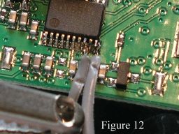
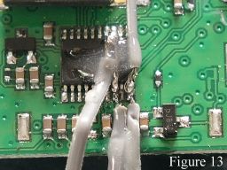
Next I needed to make connections to the pins and the pads. I have tried thin, enamelled copper wire; whilst this is nice and flexible in long lengths, in short ones it is very stiff indeed. In particular I found it too stiff to do the bridge between pins 8 and 13. This time I used wire stripped from a ribbon cable. This is multi-stranded and plastic-insulated and a little thick, but is nice and flexible. For the bridge across the IC from pin 8 to pin 13, I first ensured that the pins were bent upwards so they extended above the top of the IC, then I took a single strand from the cable, folded it in half around one pin and then the two parts round the other pin before soldering it in place. This gave me two thicknesses of wire between the pins—more than enough. For the other wires that connect to the extra circuit board, I stripped the insulation off about 2 mm of the wire, removed all but about three of the wires, twisted the others together and soldered them before attaching them to the pin or the pad. My original intention was to glue them to the board before soldering, but this didn't prove at all easy, so in the end I supported the wire in a clamp and soldered it to the pad or the pin before gluing it in place with Araldite. The glue was left to set before the board was touched again. You can see the idea in Figure 12. The final form can be seen in Figure 13.
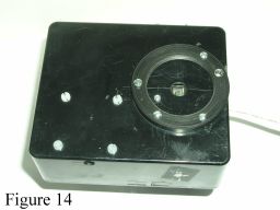 The main camera board was secured in the project box by means of two bolts through the same holes
that fixed it in its original case. I can give very little guidance on how to drill all the holes required
in just the right places. I have a 9-mm hole immediately in front of the CCD and I needed two more holes for
the bolts that hold the camera board in place. These need to be placed as accurately as possible to centre the
CCD in the 9-mm hole. Then I needed a few (I have 4 but 3 would do) holes to fix the lens ring to the front
of the box. This can be seen in Figure 14. One of the fixing screws for the camera board had to come
through under the ring, so I drilled a hole in the ring to accommodate it. This ring was made for me by a
fellow member of QCUIAG who has a lathe, and I am extremely grateful to him for that. Previously I had used
the ring from the front of an old SLR camera, but thanks to my friend I could return that to its camera.
I expect a standard SLR extension ring could be used instead.
The camera board is held by two bolts with three nuts on each; I found the best way was to fix the bolts
to the board first and then use two more nuts on each bolt to fix them to the case. Obviously the reverse
would be possible, but it is all too easy to knock a component off the circuit board whilst tightening a nut
(I know, I did it). The four other bolts seen in Figure 14 hold an internal fan (see below) and two of them
also support the secondary circuit board.
The main camera board was secured in the project box by means of two bolts through the same holes
that fixed it in its original case. I can give very little guidance on how to drill all the holes required
in just the right places. I have a 9-mm hole immediately in front of the CCD and I needed two more holes for
the bolts that hold the camera board in place. These need to be placed as accurately as possible to centre the
CCD in the 9-mm hole. Then I needed a few (I have 4 but 3 would do) holes to fix the lens ring to the front
of the box. This can be seen in Figure 14. One of the fixing screws for the camera board had to come
through under the ring, so I drilled a hole in the ring to accommodate it. This ring was made for me by a
fellow member of QCUIAG who has a lathe, and I am extremely grateful to him for that. Previously I had used
the ring from the front of an old SLR camera, but thanks to my friend I could return that to its camera.
I expect a standard SLR extension ring could be used instead.
The camera board is held by two bolts with three nuts on each; I found the best way was to fix the bolts
to the board first and then use two more nuts on each bolt to fix them to the case. Obviously the reverse
would be possible, but it is all too easy to knock a component off the circuit board whilst tightening a nut
(I know, I did it). The four other bolts seen in Figure 14 hold an internal fan (see below) and two of them
also support the secondary circuit board.
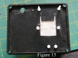
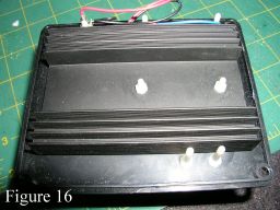
Having decided not to remove the CCD from the board, I had to cool the whole of the inside of the case.
This, I'm sure, is not nearly as effective as direct cooling to the CCD, but better than nothing I hope.
I happened to have a large heat-sink in the junk box so this is mounted inside the box with the peltier
cell sandwiched between it and a heat-sink on the outside. I cut a square hole in the lid of the box to take
the peltier (Figure 15), the extra slots being to take the wires. I think the peltier should ideally be
sealed along its edge, but I didn't know what to do that with, so decided to leave it alone. The outer
heat-sink is a standard CPU cooler with fan (cheaper bought as a unit than separately). The sandwich consists
of the CPU heat-sink, an aluminium plate, the peltier, and the internal heat-sink with heat-sink compound
between all the surfaces, and the whole thing bolted together with nylon bolts. The assembly is held in place
by more nylon bolds through the aluminium plate and the lid of the box. Power comes through a standard power
connector also mounted on the lid so that the whole assembly is self-contained on the lid of the box. The two
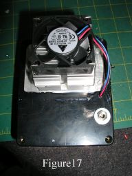
sides can be seen in Figures 16 and 17
.
In order to encourage air to circulate within the box and, I hoped, make cooling more efficient, I mounted
another small fan inside the box. This blows down onto the bottom of the box, and is secured by four nylon
bolts, which can be seen in Figure 14, with nuts under the fan to hold it just off the bottom of the box.
I felt I didn't want this going at full speed, so I provided a simple Darlington-pair transistor circuit to
reduce the voltage. It is powered from the same power source as the peltier which unfortunately means that
the lid and the box are joined by its power cable.
I found it necessary to put some insulation between the internal heat-sink and the lid of the box.
There is very little space there but I found that a couple of pieces of paper reduced the heat loss here
quite significantly.
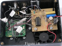 The inside of the complete camera can be seen in Figure 18. Some of the results of my "work it out
as you go along" approach to any project are visible. For example, I originally put the LED in line with the
switch and the socket, but it fouled the circuit board, so I had to move it. The original hole is sealed with
silicone sealant supported (until it set) by a piece of sticky tape. Holes to give access to the trimpots are
similarly sealed. I feel it would be worth adding more internal insulation, but to be honest I'm not sure how.
In use the box cools sufficiently for water to condense on the outside. I decided not to cut the USB cable
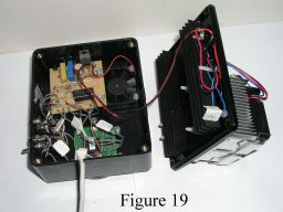
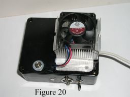
and provide a socket, so that cable comes out through a slot in the side of the box. Figure 19 shows the
camera opened up and Figure 20 the finished unit. I use an angled connector for the connection to the parallel
port for a more compact result.
The inside of the complete camera can be seen in Figure 18. Some of the results of my "work it out
as you go along" approach to any project are visible. For example, I originally put the LED in line with the
switch and the socket, but it fouled the circuit board, so I had to move it. The original hole is sealed with
silicone sealant supported (until it set) by a piece of sticky tape. Holes to give access to the trimpots are
similarly sealed. I feel it would be worth adding more internal insulation, but to be honest I'm not sure how.
In use the box cools sufficiently for water to condense on the outside. I decided not to cut the USB cable
and provide a socket, so that cable comes out through a slot in the side of the box. Figure 19 shows the
camera opened up and Figure 20 the finished unit. I use an angled connector for the connection to the parallel
port for a more compact result.
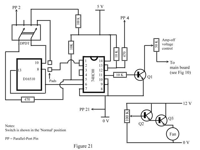 A circuit diagram for my extra circuit board is shown in Figure 21. The
observant reader will notice that, where the diagram shows 470-ohm resistors, I have used 510 ohms. There is
nothing critical about these values, 470 ohms is more common, but I didn't happen to have any so I used 510 ohms,
which I did have. The only resistor that is in any way critical is the 50K trimpot. 100K would
certainly do but not anything smaller than 50K.
A circuit diagram for my extra circuit board is shown in Figure 21. The
observant reader will notice that, where the diagram shows 470-ohm resistors, I have used 510 ohms. There is
nothing critical about these values, 470 ohms is more common, but I didn't happen to have any so I used 510 ohms,
which I did have. The only resistor that is in any way critical is the 50K trimpot. 100K would
certainly do but not anything smaller than 50K.
Transistor Q1 is Greg Beeke's Q2 and can be any npn signal
transistor. Q3 has to take the full current of the fan; I don't remember exactly what this was but it
was more than 100 mA. My Q3 is an unmarked plastic type bought many years ago as 'out of spec' and it has a very
low gain, so I had to use something rather more than a signal transistor for Q2 as well.
Most modern laptop computers only have USB ports. Experience by members of QCUIAG indicates that USB-parallel converters often do not work for this application, but USB-serial converters do work. So it is necessary to control the camera via a serial port and the writers of capture software have made provision for this.
There are however two fundamental differences between parallel and serial ports which have to be taken into account by the constructor.
1. Computers' serial ports can only control two output lines, called the RTS and DTR lines. The circuit above only requires two control lines, but some cameras, for example the Atik camera which I have, use a third line (pin 5 on the parallel port) to replace the switch shown in Figure 21, so an extra switch has to be provided for such cameras. I had to make both versions.
2. The voltages produced by the two ports are different - parallel ports produce either 0 volts or +5 volts, but serial ports produce either something between +5 and +15 volts or something between -5 and -15 volts. (My USB-serial converters produce ±6.5 volts.) The control chips in the camera are not designed for such high voltages.
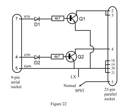
One solution to this problem is shown in Figure 22 which follows the circuit on the K3CCDTools website. None of the components is critical; the transistors, Q1 and Q2, can be any plastic npn transistor, the diodes, D1 and D2, any simple diode that can withstand -15 volts, and the resistors anything in the region of 5K. I used parts found in my junk box, the transistors and diodes were bought many years ago as unlabelled, untested devices which I tested to ensure they were functional. (The transistors are better plasic because metal ones have their collectors connected to the can, so they would need to be insulated to ensure they didn't touch anything they shouldn't.)
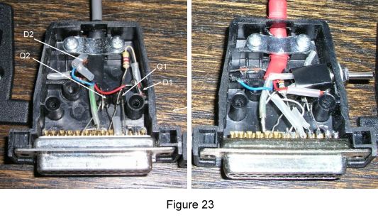
I built the circuit into the 25-pin socket cover as shown in Figure 23. I have labelled the components in one picture, most of them are hidden by the switch in the other. Most of the connections are covered with heat-shrink tubing to ensure that they don't touch anything they shouldn't when the cover is put in place (I also slipped a piece of tape under the red wire for the same reason). The centre wire of the transistors is the base connection and is folded back and soldered directly to the resistor; the emitter and collector leads are soldered directly to the connector. The other components are simply arranged to fit inside the cover. It is important that the exit cable is firmly secured by means of the clamp provided with the shell. The cable is screened and uses the screen as the earth connecton. I've not shown the 9-pin connector because this simply has the red wire connected to pin 7, the blue to pin 4, and the screen to pin 5.
Home Back to the Equipment